Photo etching is a chemical milling process used for the manufacture of metal with the help of a photoresist and etching solutions. The technology appeared in the 60s of the 20th century and was initially used in the manufacture of printed circuit boards. Photo etching is an economical alternative to stamping, laser and hydraulic cutting. All active components and equipment are relatively cheap, so the technology is widely used in mass production (for example, in the manufacture of inscriptions and logos).
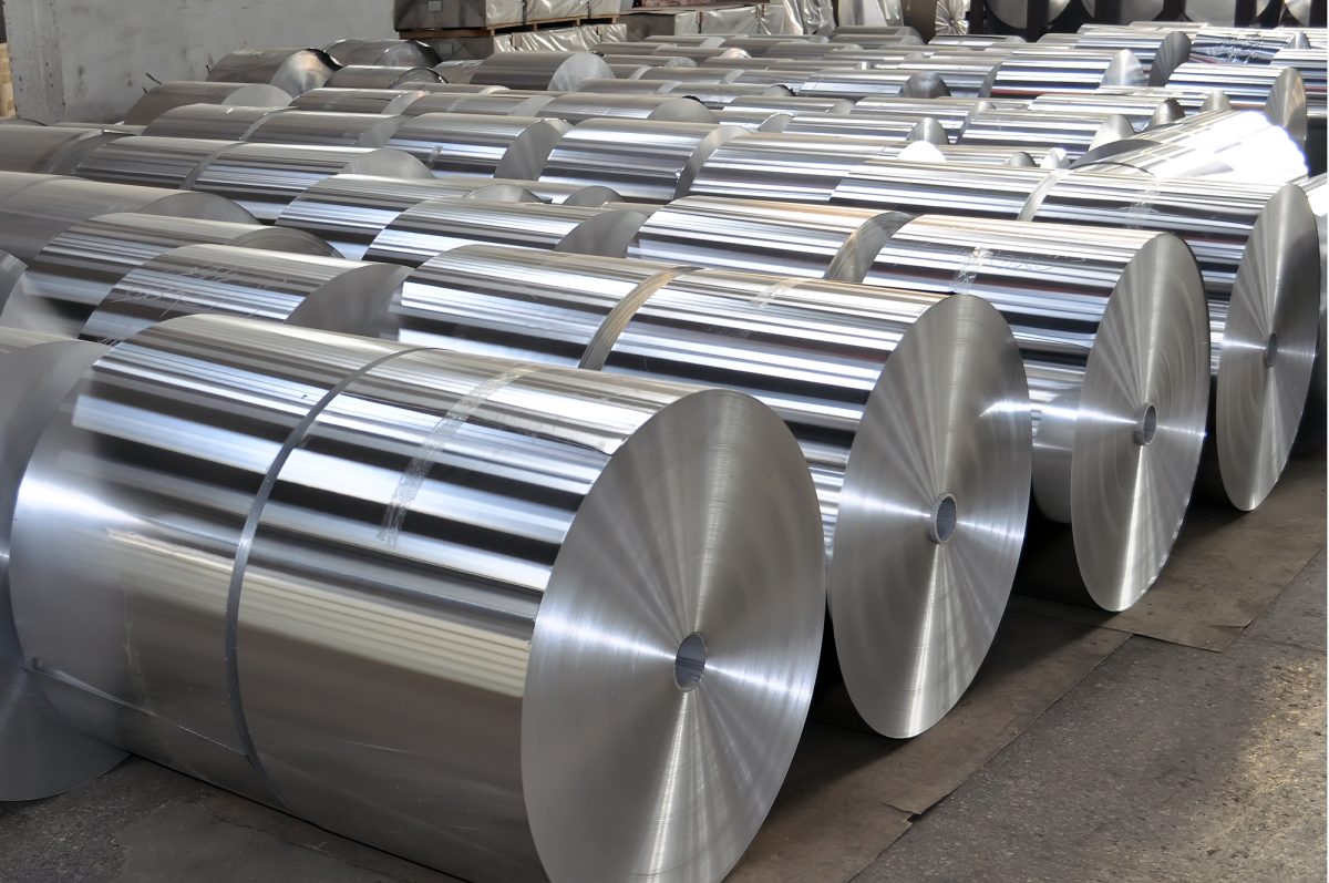
Metals such as brass, copper, aluminum, nickel, stainless steel, manganese, zinc, titanium and silver are used as materials for photo etching. The thickness of the metal plates used as blanks varies from 0.013 to 2 mm.
Photo etching in modelling involves the use of a technique of chemical etching of elements from a metal sheet (no more than one and a half millimeters thick). Copper alloys or ordinary copper act as the base material. Photo etching kits allow to replace oversized elements that cannot be carefully made of polymer materials.
There are many options for photo etching, involving the use of various equipment, tools, materials and chemicals. The entire technological process is divided into several stages:
- creating a photo template,
- preparation of the material,
- exposure,
- development,
- etching

